Diagram Of PCBs
What are Printed Circuit Boards?
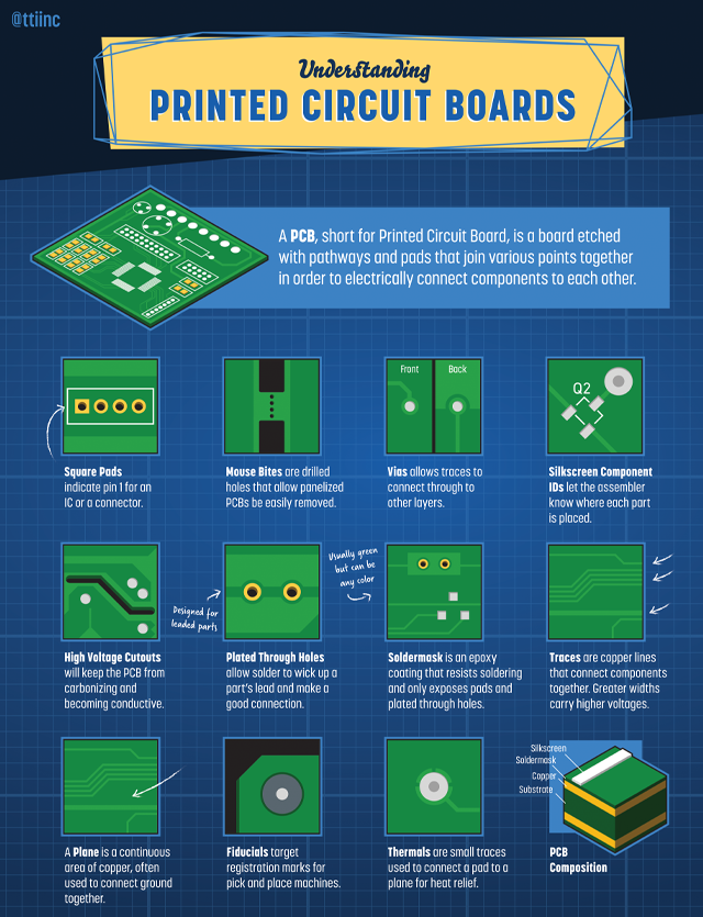
A PCB, short for Printed Circuit Board, is a board etched with pathways and pods that join various points together in order to electronically connect components to each other.
A Printed Circuit Board's design functionality:
Square Pods indicate pin 1 for an IC or a connector.
Mouse Bites are drilled holes that allow panelized PCBs to be easily removed.
Vias allow traces to connect to other layers.
Silkscreen Component IDs let the assembler know where each part is placed.
High Voltage Cutouts will keep the PCB from carbonizing and becoming conductive.
Plated Through Holes allow the solder to wick up a part’s lead and make a good connection, also designed for leaded parts.
Soldermasks is an epoxy coating that resists soldering and only exposes pads and plated through holes, it’s usually green but can be any color.
Traces are copper lines that connect components together. Greater widths carry higher voltages.
A Plane is a continuous area of copper, often used to connect ground together.
Fiducials target registration marks for pick and place machines.
Thermals are small traces used to connect a pad to a plane for heat relief.
PCB Composition in order consists of a top silkscreen, a soldermask with a copper layer underneath, following a substrate layer.
Looking for Printed Circuit Boards? Search TTI's Inventory